


Screen Holdings is a corporate group based in Kyoto that was originally established as a printer in 1868. The group now offers solutions in markets ranging from printing and display screens to semiconductors and printed circuit boards, anchored by its two core technologies: surface control and processing, and imaging and patterning.
Screen Semiconductor Solutions Co. Ltd. is part of Screen Holdings, which specializes in semiconductor manufacturing equipment, including wafer-cleaning systems. The company focuses on ultraclean, fluid control and drying technologies to support the crucial step of surface treatment in semiconductor fabrication, which ensures that all microscopic impurities are removed.
Semiconductor manufacturing consumes vast amounts of energy, water and chemicals, so reducing the environmental impact is viewed as an urgent task. Screen is tackling this challenge head-on by integrating environmental initiatives into its business strategy, with the aim of promoting a sustainable society while improving its corporate value.
In a recent interview with The Japan Times, four employees discussed the company’s ongoing efforts to uphold its strong commitment to sustainability.
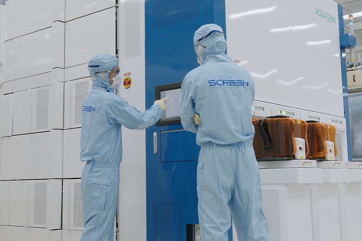
Reducing greenhouse gas emissions
Screen has set a goal of achieving carbon neutrality by 2050. Its efforts include lowering carbon dioxide output at its factories, which fall under Scope 1 (direct emissions) and Scope 2 (indirect emissions from purchased energy) of the GHG Protocol, an international standard for measuring and managing GHG emissions.
Screen’s initial goal, set in April 2020, was aligned with the global target set out by the Paris Agreement, which aims to limit global warming to “well below 2 degrees” above preindustrial levels. Based on this target, the company received certification from the Science Based Targets initiative.
“However, as the global consensus shifted toward the new 1.5-degree target, we decided to accelerate our efforts and underwent recertification in January 2024 based on the new goal,” said Kumiko Fukue, manager of the Environmental Management Section in Screen Holdings’Ìý Sustainability Promotion Department.
To do this, the company decided to start using renewable energy at its major sites in Japan ahead of schedule.
“We had originally set a target to start using renewable energy at all our major sites by 2027, but we achieved this in early 2025 instead,” Fukue said.
As a result of these proactive efforts, the company achieved a 56.6% reduction in Scope 1 and 2 emissions from business activities in fiscal 2025, which ended in March, from its emission levels in March 2019. This represents significant progress toward its goal of slashing emissions by 70% by the end of the fiscal 2027.
At the Hikone Site, the company’s main manufacturing factory, renewable energy was introduced in fiscal 2022. In addition, energy-efficient equipment became standard for new factories. This includes task and ambient air conditioning, which cools only areas where human activity is present.
Green product strategy
When it comes to corporate efforts, lowering the carbon emissions generated by the use of a company’s products — known as Scope 3, Category 11 under the GHG Protocol — is crucial. This is important not only for gauging a company’s overall environmental impact, but also for helping its customers reduce emissions.
In addition to making constant improvements to its products, Screen has changed the basis on which it calculates Scope 3 Category 11 emissions, shifting from a total mass basis to a per-unit-of-gross-profit basis.
“This is an attempt to pursue business growth and reduce greenhouse gas emissions simultaneously,” said Tomoko Kitazaki of the Environmental Management Section of the Sustainability Promotion Department.
By focusing on how much carbon dioxide is emitted per million yen of gross profit, rather than merely looking at the total emissions, the company expects to strengthen the link between its business strategy and sustainability efforts.
Screen has its own environmental standards for product development and certifies products that meet these criteria as “Green Products.” The criteria span six categories — energy savings, resource conservation, ease of disassembly, reuse of resources, environmental protection and safety, and availability of information.
“For fiscal 2024, Green Products accounted for over 90% of total equipment sales,” Kitazaki said.
Others are labeled “Super Green Products” if they meet the previous criteria and achieve GHG emissions of at least 30% per unit of processing area versus products sold in fiscal 2019 as a base line. The aim is to increase sales of these environmentally superior products to 3% by the end of fiscal 2027.
These efforts have contributed immensely to reducing Scope 3, Category 11 emissions. The target was to achieve a 48% reduction per unit of gross profit for fiscal 2027, but the company easily surpassed that with a 55.7% cut in 2025 — more than two years ahead of schedule.
Reducing water usage
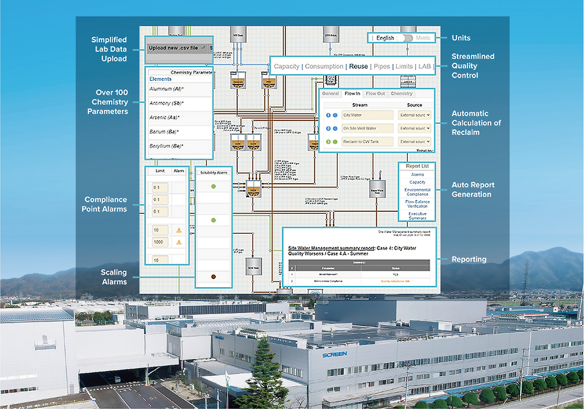
Screen has been working with FTD Solutions since 2023 to adopt a water management application that visualizes its water usage.
The first step was to carry out a highly advanced verification process at the Hikone Site. Jun Shibukawa of the ESG (environmental, social and governance) Promotion Department of Screen Semiconductor Solutions said this process provided valuable insights.
“First, we identified opportunities to reduce water usage. We clarified areas where water could be reused, such as for cooling compressors, and mapped out the reuse process,” he said.
Based on this initial assessment, the company developed a strategic model incorporating various measures to reduce water usage, including by reusing compressor cooling water. The effectiveness of this approach was then verified, confirming that a plant’s water intake can be reduced substantially.
“At the Hikone Site, we are installing more flow meters to enable us to continuously monitor key performance indicators such as water usage, drainage and reuse rates. This will help to improve the accuracy of our model,” Shibukawa said.
The company is looking to eventually use these water management insights to provide water-saving solutions to its customers as well.
Optimizing wafer cleaning
As semiconductors become tinier and more complex, the wafer-cleaning process requires greater cleaning capabilities and a large quantity of extremely pure water. Furthermore, the temperature of this water must be strictly controlled.
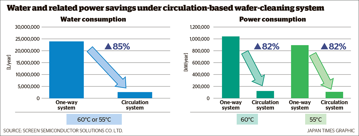
With conventional equipment, ultrapure water flowed constantly and was subsequently discharged — even when no wafers were being processed — to maintain the required temperature and purity. “To minimize water usage, we developed an ultrapure water circulation unit that filters and cleans the water,” Shibukawa said.
The water is then reheated and supplied to the equipment only when needed, optimizing energy-efficiency as well. This new system helped Screen slash water-related power use by 82%.
Shibukawa noted that the demand for water-reduction capabilities is high among water-conscious customers, especially in Taiwan, one of the world’s major chip suppliers.
Moreover, in an era focused on sustainability, companies are constantly facing demands to make greater contributions to the cause. This trend influences the decisions manufacturers make on machinery and materials, which means that Screen’s technology for optimizing water and power usage is a crucial part of its international business strategy. In fact, Screen’s pure water circulation function has already been incorporated into its current products.
The company is also making advances in developing functions to circulate and reuse wafer-cleaning chemicals, which are both financially and environmentally costly.
This technology has already been adopted to handle certain cleaning solutions and can be used by modifying existing equipment. However, this is a highly challenging technology that must be updated constantly.
Since there are various kinds of cleaning processes for different types of semiconductors, each requires the use of specific chemical solutions at concentrations that must be strictly controlled, Shibukawa said.
“Sometimes several chemicals need to be mixed. In such cases, we first need to separate the mixed chemicals before processing them to be ready for reuse. We are continuing to develop this technology to increase the variety of chemicals it can handle,” Shibukawa said.
He also emphasized that none of these developments would be possible without the participation and support of stakeholders in the semiconductor supply chain.
“For example, the water filters installed in our equipment are made by a filter manufacturer, not by us. We need to work closely with such suppliers to ensure that we share the same standards regarding the cleanliness of our plants and the precision of our products, because that is what creates our value,” he said.
Connecting with communities
While expanding internationally, Screen places great importance on coexisting and prospering with the communities where the company operates.
In Kyoto, where the company was founded, it conducts and participates in activities designed to contribute to the region as a whole.
One such activity is the Kyoto Model Forest, a grassroots initiative led by the Kyoto Model Forest Association to protect and nurture the area’s forestry assets. Through this initiative, Screen has subsidized forest maintenance costs in the western Kyoto suburb of Kameoka since 2018 and held events aimed at improving the public’s understanding of biodiversity.
Participation in this movement led to a comprehensive partnership agreement for regional revitalization being signed between the company and the Kyoto Prefectural Government, which supports the company’s deeper and broader efforts at community engagement.
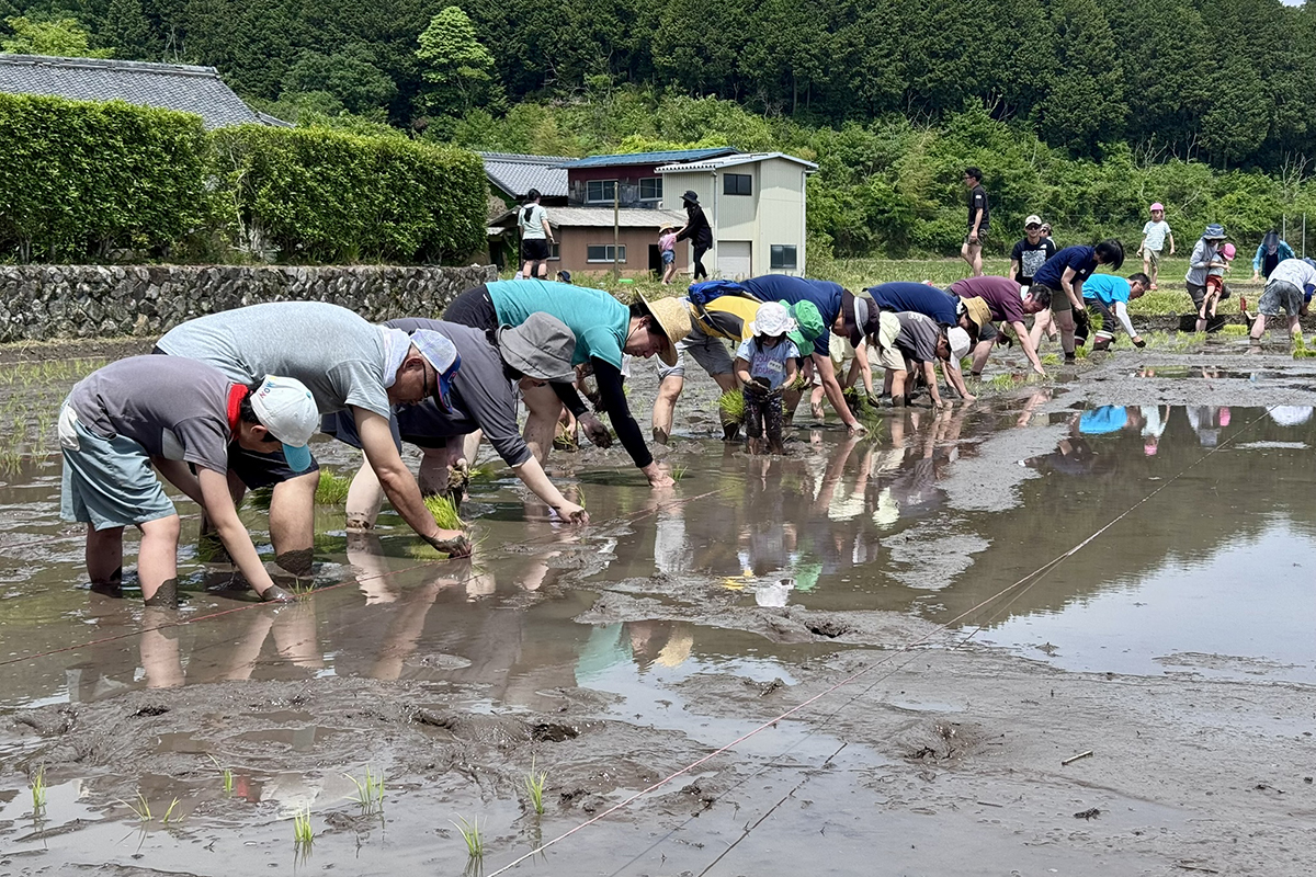
Since 2018, the company’s employees have participated in rice-growing activities.
“This year, too, a lot of our employees and their family members joined residents in planting rice seedlings in May and harvesting the rice in September,” Fukue said.
The harvested rice was initially donated to a Kameoka children’s home, but now it is delivered to multiple children’s homes throughout the prefecture. Fukue said Screen will continue this initiative, calling it a valuable activity that vitalizes community exchanges and helps the people.
Becoming indispensable
Screen’s sustainability strategy aims to promote well-being by simultaneously driving efforts to reduce the environmental impact of its factories and products while contributing to the communities in which it operates.
Engaging the various stakeholders will establish the company as a leader in pursuing sustainability within the semiconductor industry, said Kyosuke Yasaka, manager of the ESG Promotion Department at Screen Semiconductor Solutions.
“Semiconductors are indispensable to the world. Both their production volume and usage will only continue to increase in the future. Furthermore, as miniaturization and stacking technologies advance, the number of steps in the semiconductor manufacturing process will increase exponentially. Consequently, the consumption of energy and water necessary for the manufacturing will also increase,” Yasaka said.
That is precisely why the entire semiconductor industry must share the common goal of achieving a sustainable society. Screen recognizes that the role of chip equipment manufacturers is a particularly important one in a world besieged by environmental stress.
“We, as manufacturing equipment makers, aim to lead the industry-wide reduction of environmental impact, thereby contributing to the sustainability of a society that relies on semiconductor technology and the environment,” Yasaka said.
This article is sponsored by Screen Semiconductor Solutions Co. Ltd.
50 years of manufacturing innovation
by AKIHIKO OKAMOTO
REPRESENTATIVE DIRECTOR AND PRESIDENT OF SCREEN SEMICONDUCTOR SOLUTIONS CO. LTD.
This year marks the 50th anniversary of our entry into the semiconductor production equipment business. Our cumulative cleaning equipment shipments surpassed 15,000 units this year. From the cutting edge of innovation to legacy nodes, these systems are being used in a variety of manufacturing processes. These milestones are thanks to the support of our customers, partners and other stakeholders. We are deeply grateful.
Recently, we decided to open a new research and development site in New York to reinforce our elemental technology and product development capabilities.
This site will be called the Screen Advanced Technology Center of America. ATCA will be set up at a clean-room facility that is part of the cutting-edge R&D facilities operated by our partner NY Creates.
We plan to install chip equipment covering a wide range of leading-edge technologies, from wafer cleaning — in which we boast the top global market share — to annealing and advanced packaging.
Working within an environment that enables evaluations of the entire sequence of cutting-edge device manufacturing processes, we expect to shorten elemental technology and product development times, further strengthen product competitiveness, and increase value.
Please look at Screen’s initiatives and let us know what you think.
Innovation, from Kyoto to the world.
We look forward to your continued partnership.


